

Maximum quantity allowed is 999
请选择数量
Fabrication and Evaluation of Organic Field-Effect Transistors (OFETs) : [70]PCBM
![[70]PCBM[P2683]](/structure-300/P2683.jpg)
[6,6]-Phenyl-C71-butyric Acid Methyl Ester (mixture of isomers)
[for organic electronics]
[70]PCBM (mixture of isomers)
CAS RN: 609771-63-3
Product Number: P2683
Performance of [70]PCBM[P2683]-based OFETs
![Performance of [70]PCBM[P2683]-based OFETs](/assets/cms-images/P2683-device-method-structure-en.png)
Table. OFETs Characteristics of [70]PCBM[P2683]-based OFETs
| Entry | Fabrication Method | Device Configuration | SAM Treatment | Polarity | μ (cm2 V−1 s−1) | Vth (V) | Ion/Ioff |
|---|---|---|---|---|---|---|---|
| Entry1 | Fabrication MethodSpin-coating | Device ConfigurationTCBG | SAM TreatmentHMDS | Polarityn | μ (cm2 V−1 s−1)2.5 × 10⁻² | Vth (V)8.8 | Ion/Ioff104 |
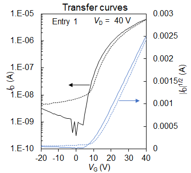
Figure. Transfer curves in the saturated region
Experimental details
Fabrication and evaluation of spin-coated [70]PCBM[P2683]-based OFETs
< Substrate>
< Self-Assembly Monolayer (SAM) Treatment>
< Spin-Coating>
< Vacuum Deposition>
< Device configuration>
< Evaluation condition>
< Substrate>
- HMDS-treated Si/SiO2 (thickness of SiO2: 200 nm)
< Self-Assembly Monolayer (SAM) Treatment>
- 1,1,1,3,3,3-Hexamethyldisilazane (HMDS) [H0089]
- Piranha etching (H2SO4:H2O2=4:1, 80ºC, 2h)
- Ultrasonication (Deionized water, Acetone, IPA, 10 min each)
- Exposure to vapor (IPA, 3 min)
- UV/O3 treatment (1 h)
- Immersion in HMDS (16 h, N2)
- Ultrasonication (Toluene, Acetone, IPA, 10 min each)
< Spin-Coating>
- [70]PCBM[P2683], 15 mg/ml, Chloroform
- Spin-coating condition: 2000 RPM, 60 sec, N2
< Vacuum Deposition>
- Deposition rate of Au: 0.2 Å/s (under a pressure of∼10−4 Pa)
< Device configuration>
- [n+-Si/SiO2 (200 nm) / [70]PCBM[P2683] / Au (40 nm)]
- Top-Contact Bottom-Gate Type (TCBG)
- Channel Length: 50 μm
- Channel width: 1.5 mm
< Evaluation condition>
- Under N2
- Field-effect mobilities (μ) were determined from the transfer curves in the saturation regime using the following equation:ID = (W/2L) μ Ci (VG − Vth)2