

Make sure to sign up for an account today for exclusive coupons and free shipping on orders over $75!
Maximum quantity allowed is 999
Please select the quantity
Morphology Control using “6P” for Performance Improvement of OFET

Features of 6P
• Applicable to light-emitting devices due to its strong blue fluorescence
• Performance improvement of OFETs by inserting 6P layer under the active laye
p-Sexiphenyl (6P), in which six benzene rings are linked at para positions, exhibits strong blue fluorescence and high thermal stability, and has been applied to organic light-emitting devices.1) Figure 1 shows absorption and emission spectra for 6P. Due to its unique self-assembling ability originating from its rigid rod-like molecular structure, 6P can form nanofibers under various conditions.2) It has been reported that insertion of a 6P layer can improve the morphology of overlying organic semiconductor layers and increase the performances of organic field effect transistor (OFET) devices.3,4)
TCI has commercialized high-purity 6P[S0220] with minimal variation between lots. We demonstrated OFET performance improvements by inserting a 6P layer blow the rubrene [T2233] or DBTTT [D5083] active layer. We also verified performance improvements using 5P [Q0018] and BP1T [B3441].
![Figure 1. Absorption and emission spectra of 6P [S0220] in thin film](/assets/cms-images/S0220-article-fig1-en.png)
Figure 1. Absorption and emission spectra of 6P [S0220] in thin film
Performance improvements of rubrene- and DBTTT-based OFETs by inserting 6P layer
To evaluate the effect of inserting a 6P layer, we fabricated rubrene- and DBTTT-based top-contact bottom-gate OFETs on thermally oxidized silicon wafers. The performance of these devices with and without a 6P layer is summarized in Fig. 2 and Table 1. In the case of the rubrene-based OFET (Fig 2b), the on-state current was enhanced by inserting the 6P layer, and the hole mobility was increased by a factor of more than 150 times. This performance improvement is higher than that achieced by a general surface treatment using an alkyl silane coupling agent. For the DBTTT-based OFET, the on-state current was also enhanced by insertion of 6P (Fig 2c). The average hole mobility was improved more than 17 times, and a maximum hole mobility of 4.4 cm2V-1s-1 was obtained.
The surface morphologies of the 6P and DBTTT layers were investigated by atomic force microscopy (AFM). As shown in Fig 3a, 6P layer exhibited an island structure on top of a flat sheet-like structure. This indicates that the 6P grains grow two-dimensionally and form successive molecular layers as the deposition amount increase. Figures 3b and 3c compare the morphologies of DBTTT layers grown without and with a bottom 6P layer, respectively. It can be seen that the use of a 6P layer reduced the number of grain boundaries without greatly affecting the grain structure. Therefore, the 6P layer can greatly improve OFET performance by suppressing structural defects in the organic semiconductor layer that hinder carrier transport.
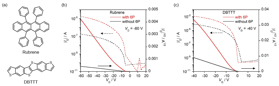
Figure 2. (a) Molecular structures of rubrene and DBTTT, (b) Transfer curves of rubrene-based OFETs, and (c) DBTTT-based OFETs

Figure 3. AFM images (5µm × 5µm) (a) 6P, (b) DBTTT, (c) 6P / DBTTT
Performance improvements of DBTTT-based OFETs by inserting 5P and BP1T layers
To investigate the effect of the type of material inserted, 5P, which has one less benzene ring than 6P, and BP1T, in which the central benzene ring in 5P is replaced by a thiophene ring, were used to fabricate DBTTT-based OFETs. The performances of these devices are shown in Fig. 4 and Table 1.The use of both 5P and BP1T led to an increase in the on-state currents, again indicating an improvements in the morphology of the DBTTT layer. However, while 6P caused a stable performance with little variation between devices, 5P and BP1T gave rise to lager variations in hole mobility, as indicated by the standard deviation in Table 1. A maximum hole mobility of 6.34cm2V-1s-1 was achieved for 5P. These results suggest that the performance may be improved by further optimization of materials and device structures.

Figure 4. (a) molecular structures of 6P, 5P, BP1T, (b) transfer curves of DBTTT-based OFETs
Table 1. Summary of OFET performance
The values in parentheses are standard deviations.
OFET device fabrication procedure
- Ultrasonic cleaning of Sin++ / SiO2 (200 nm) substrate (Acetone, IPA 10 minutes each)
- Boiling cleaning (IPA, 3min)
- UV/O3 cleaning (20min)
- Vacuum deposition of 6P [S0220] or 5P [Q0018] or BP1T [B3441] (described in bellow)
- Vacuum deposition of DBTTT [D5086] or Rubrene [T2233] (described in bellow)
- Vacuum deposition of Au electrode (thickness: 40 nm, channel length: 50 μm, channel width: 1.5 mm)
- Storage in the vacuum chamber overnight.
- Device performance evaluation in a nitrogen glove box.
Vacuum deposition procedure of organic material
< 6P [S0220], 5P [Q0018], BP1T [B3441] >- Substrate temperature during deposition: 140°C
- Deposition rate: 0.1Å/sec
- Film thickness: 8 nm
- Substrate temperature during deposition: 25°C
- Deposition rate: 0.15Å/sec
- Film thickness: 60 nm
- Substrate temperature during deposition: 25°C
- Deposition rate: 0.5Å/sec
- Film thickness: 40 nm
References
1) S. Tasch, C. Brandstätter, F. Meghdadi, G. Leising, G. Froyer, L. Athouel, Adv. Mater., 1997, 9, 33.2) C. Simbrunner, Semicond. Sci. Technol., 2013, 28, 053001.
3) X. Qian, T. Wang, D. Yan, Appl. Phys. Lett, 2013, 103, 173512.
4) A. Choi, Y.-N. Kwon, J. W. Chung, Y. Yun, J.-Il Park, Y. U. Lee, AIP Advances, 2020, 10, 025127.
Related Products
Material purity is an important factor directly influencing their OFET device parameters.
To check and enhance the quality and purity of the transistor materials, TCI has recently begun the fabrication and evaluation of the OFET devices using our products. We always seek to improve our technology and skill in order to provide high-purity and quality materials.