

Make sure to sign up for an account today for exclusive coupons and free shipping on orders over $75!
Maximum quantity allowed is 999
Please select the quantity
Fabrication and Evaluation of Organic Field-Effect Transistors (OFETs) : Fullerene C60
![Fullerene C60 (purified by sublimation) [for organic electronics] [F1232]](/structure-300/F1232.jpg)
Fullerene C60 (purified by sublimation) [for organic electronics]
CAS RN: 99685-96-8
Product Number: F1232
Performance of Fullerene C60 [F1232]-based OFETs
![Fabrication method and evaluation of vacuum-deposited C60 [F1232]](/assets/cms-images/F1232-device-method-structure-en.png)
Table. Characteristics of Fullerene C60 [F1232]-based OFETs
| Entry | Fabrication Method | Device Configuration | SAM Treatment | Tsub (°C) | Polarity | μ (cm2 V−1 s−1) | Vth (V) | Ion/Ioff |
|---|---|---|---|---|---|---|---|---|
| Entry1 | Fabrication MethodVacuum Deposition | Device ConfigurationTCBG | SAM TreatmentHMDS | Tsub (°C)RT | Polarityn | μ (cm2 V−1 s−1)0.27 | Vth (V)18.8 | Ion/Ioff106 |
| Entry2 | Fabrication MethodVacuum Deposition | Device ConfigurationTCBG | SAM TreatmentOTS | Tsub (°C)RT | Polarityn | μ (cm2 V−1 s−1)0.51 | Vth (V)16.1 | Ion/Ioff106 |
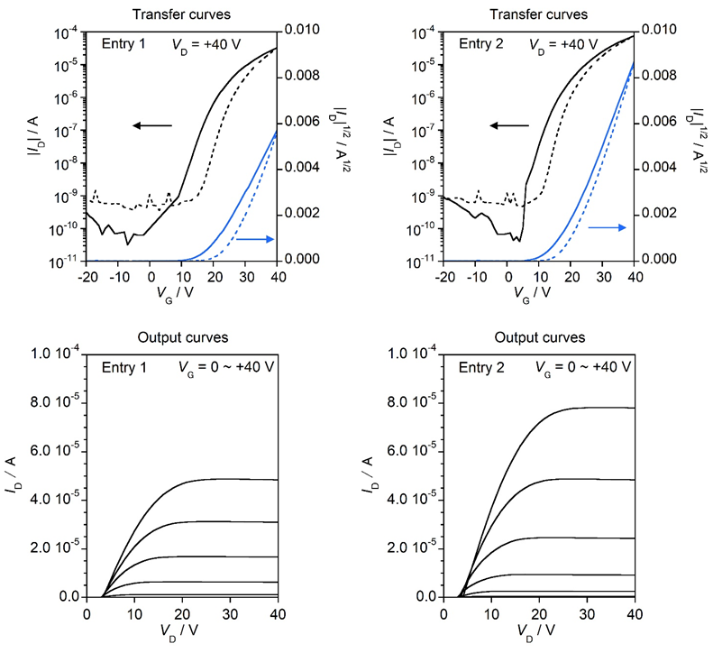
Figure. Transfer curves in the saturated region and output curves at different gate voltages
Experimental details
Fabrication and evaluation of spin-coated Fullerene C60 [F1232]-based OFETs
< Substrate >
< Self-Assembly Monolayer (SAM) Treatment >
< Vacuum Deposition >
< Device Configuration >
< Evaluation Condition >
< Substrate >
- HMDS-treated Si/SiO2 (thickness of SiO2:200 nm)
- OTS-treated Si/SiO2 (thickness of SiO2:200 nm)
< Self-Assembly Monolayer (SAM) Treatment >
- 1,1,1,3,3,3-Hexamethyldisilazane (HMDS) [H0089]
- Piranha etching (H2SO4:H2O2=4:1, 80 ºC, 2 h)
- Ultrasonication (Deionized water, Acetone, IPA, 10 min each)
- Exposure to vapor (IPA, 3 min)
- UV/O3 treatment (1 h)
- Immersion in HMDS (16 h, N2)
- Ultrasonication (Toluene, Acetone, IPA, 10 min each)
- n-Octyltrichlorosilane (OTS) [O0168]
- Piranha etching (H2SO4:H2O2=4:1, 80 ºC, 2 h)
- Ultrasonication (Deionized water, Acetone, IPA, 10 min each)
- Exposure to vapor (IPA, 3 min)
- UV/O3 treatment (1 h)
- Immersion in OTS solution (0.01 M toluene, 16 h, N2)
- Ultrasonication (Toluene, Acetone, IPA, 10 min each)
< Vacuum Deposition >
- Deposition rate of Fullerene C60 [F1232]: 0.15 Å/s (under a pressure of∼10−4 Pa)
- Substrate temperature during deposition: RT
- Deposition rate of Au: 0.2 Å/s (under a pressure of∼10−4 Pa)
< Device Configuration >
- [n+-Si/SiO (200 nm) / Fullerene C60 [F1232] (40 nm) / Au (40 nm)]
- Top-Contact Bottom-Gate Type (TCBG)
- Channel Length: 50 μm
- Channel width: 1.5 mm
< Evaluation Condition >
- Characteristics of OFET devices were measured in a nitrogen glove box.
- Field-effect mobilities (μ) were determined from the transfer curves in the saturation regime using the following equation:
ID = (W/2L) μ Ci (VG − Vth)2