Maintenance Notice (3:15 - 7:30 AM February 22, 2025 UTC): This website is scheduled to be unavailable due to maintenance. We appreciate your patience and understanding.
Notice of Discontinuing the Use of Password-Protected Compressed Files | Product Document Searching Made Easy by 2D Code! | TCI Life Science News February 2025 | [Product Highlights] Chemiluminescent Reagents for... | Various analytical charts can be searched on each product detail page and Product Document Search (The kinds of analytical charts differ by product)
Maximum quantity allowed is 999
Please select the quantity
Fabrication and Evaluation of Organic Field-Effect Transistors (OFETs) : Fullerene C60
![Fullerene C60 (purified by sublimation) [for organic electronics] [F1232]](/structure-300/F1232.jpg)
Fullerene C60 (purified by sublimation) [for organic electronics]
CAS RN: 99685-96-8
Product Number: F1232
Performance of Fullerene C60 [F1232]-based OFETs
![Fabrication method and evaluation of vacuum-deposited C60 [F1232]](/assets/cms-images/F1232-device-method-structure-en.png)
Table. Characteristics of Fullerene C60 [F1232]-based OFETs
| Entry | Fabrication Method | Device Configuration | SAM Treatment | Tsub (°C) | Polarity | μ (cm2 V−1 s−1) | Vth (V) | Ion/Ioff |
|---|---|---|---|---|---|---|---|---|
| Entry1 | Fabrication MethodVacuum Deposition | Device ConfigurationTCBG | SAM TreatmentHMDS | Tsub (°C)RT | Polarityn | μ (cm2 V−1 s−1)0.27 | Vth (V)18.8 | Ion/Ioff106 |
| Entry2 | Fabrication MethodVacuum Deposition | Device ConfigurationTCBG | SAM TreatmentOTS | Tsub (°C)RT | Polarityn | μ (cm2 V−1 s−1)0.51 | Vth (V)16.1 | Ion/Ioff106 |
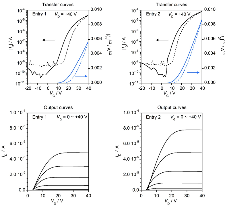
Figure. Transfer curves in the saturated region and output curves at different gate voltages
Experimental details
Fabrication and evaluation of spin-coated Fullerene C60 [F1232]-based OFETs
< Substrate >
< Self-Assembly Monolayer (SAM) Treatment >
< Vacuum Deposition >
< Device Configuration >
< Evaluation Condition >
< Substrate >
- HMDS-treated Si/SiO2 (thickness of SiO2:200 nm)
- OTS-treated Si/SiO2 (thickness of SiO2:200 nm)
< Self-Assembly Monolayer (SAM) Treatment >
- 1,1,1,3,3,3-Hexamethyldisilazane (HMDS) [H0089]
- Piranha etching (H2SO4:H2O2=4:1, 80 ºC, 2 h)
- Ultrasonication (Deionized water, Acetone, IPA, 10 min each)
- Exposure to vapor (IPA, 3 min)
- UV/O3 treatment (1 h)
- Immersion in HMDS (16 h, N2)
- Ultrasonication (Toluene, Acetone, IPA, 10 min each)
- n-Octyltrichlorosilane (OTS) [O0168]
- Piranha etching (H2SO4:H2O2=4:1, 80 ºC, 2 h)
- Ultrasonication (Deionized water, Acetone, IPA, 10 min each)
- Exposure to vapor (IPA, 3 min)
- UV/O3 treatment (1 h)
- Immersion in OTS solution (0.01 M toluene, 16 h, N2)
- Ultrasonication (Toluene, Acetone, IPA, 10 min each)
< Vacuum Deposition >
- Deposition rate of Fullerene C60 [F1232]: 0.15 Å/s (under a pressure of∼10−4 Pa)
- Substrate temperature during deposition: RT
- Deposition rate of Au: 0.2 Å/s (under a pressure of∼10−4 Pa)
< Device Configuration >
- [n+-Si/SiO (200 nm) / Fullerene C60 [F1232] (40 nm) / Au (40 nm)]
- Top-Contact Bottom-Gate Type (TCBG)
- Channel Length: 50 μm
- Channel width: 1.5 mm
< Evaluation Condition >
- Characteristics of OFET devices were measured in a nitrogen glove box.
- Field-effect mobilities (μ) were determined from the transfer curves in the saturation regime using the following equation:
ID = (W/2L) μ Ci (VG − Vth)2