

Maintenance Notice (5:15 AM - 4:55 PM May 24, 2025): This website is scheduled to be unavailable due to maintenance. We appreciate your patience and understanding.
Published TCIMAIL newest issue No.198
Maximum quantity allowed is 999
Features of S-DNTT-10
• High hole mobility > 10 cm2/Vs (Dip-coating method)
• Applicable to both dry and wet processes
• High durability

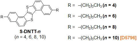
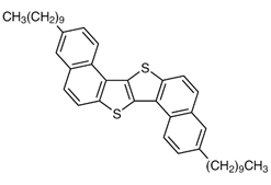
Figure2. Chemical structures of S-DNTT-n
Table1. Summary of physical property data1)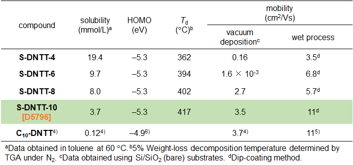
TCI has commercialized an excellent p-type semiconductor material, S-DNTT-10 [product number: D5796]. We have begun fabrication and evaluation of OFET devices in our laboratory. Please see below for the details.
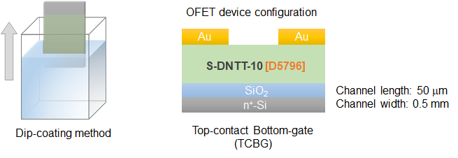
Figure3. OFET device fabrication method and device configuration
Device fabrication procedure
Semiconductor layers (thickness = 30−50 nm) of S-DNTT-n (n = 4, 6, 8, 10) were formed on bare Si/SiO2 substrates (SiO2: 200 nm) by dip-coating method (pulling rate: 4 μm/sec) from their toluene solutions (1.0 g/L, 50 °C) under a nitrogen atmosphere. The top-contact type OFETs were completed by depositing gold (thickness = 40 nm) as source and drain electrodes (Figure 3).
Device performance
Performance of the OFET devices are summarized in Table 2. All S-DNTT-n (n = 4, 6, 8, 10) exhibited typical p-type semiconductor characteristics. The mobilities of S-DNTT-n are strongly dependent on their alkyl chain lengths. The S-DNTT-10-based OFET device showed the highest transport performance with a mobility of 11 cm2/Vs (Figure 4a). In addition, we have conducted cycle measurement as a durability test using the S-DNTT-10-based device. Even after a series of 100 cycles, the device maintained its stable transistor operation, indicating almost no performance deterioration (Figure 4b). We have demonstrated that S-DNTT-10 is an excellent semiconductor material which possesses both good air stability and durability.
Table2. Characteristics of dip-coated OFETs based on S-DNTT-n1)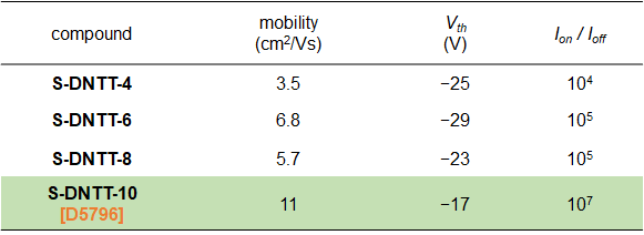
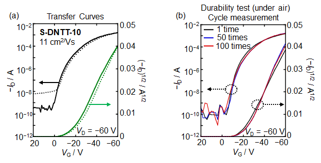
Figure4. Performance of dip-coated OFETs based on S-DNTT-101)
(a) Transfer curves (b) Cycle measurement under air

Figure5. OFET device fabrication method and device configuration
Device fabrication procedure
Semiconductor layers (thickness = 50−100 nm) of S-DNTT-n (n = 4, 6, 8, 10) were formed on bare Si/SiO2 substrates (Si/SiO2: 200 nm) at room temperature by vacuum deposition method. The top-contact type OFETs were completed by depositing gold (thickness = 40 nm) as source and drain electrodes (Figure 5).
Device performance
Performance of the OFET devices are summarized in Table 3. All S-DNTT-n (n = 4, 6, 8, 10) exhibited typical p-type semiconductor characteristics. The obvious improvement of transistor performance was observed in each S-DNTT-n-based device by post-annealing treatment (Table 3). In addition, the mobilities of S-DNTT-n are strongly dependent on their alkyl chain lengths. The S-DNTT-10-based OFET device showed the highest transport performance with a mobility of 3.5 cm2/Vs (Table 3 and Figure 6).
Table3. Characteristics of vacuum-deposited OFETs based on S-DNTT-n1)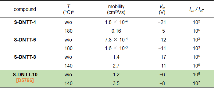
aPost-annealing temperature.
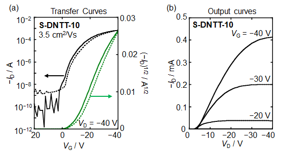
Figure6. Performance of vacuum-deposited OFETs based on S-DNTT-101)
(a) Transfer curves (b) Output curves