

It has come to our notice that certain fraudulent individuals or entities are misusing our Company’s name and TCI’s registered trademarks by promoting and offering regulated and hazardous chemical substances through online platforms like YouTube. We hereby categorically clarify that TCI has no association or connection whatsoever with the products being displayed or sold in the videos. These products have been falsely represented as being associated with TCI, and the unauthorized use of our trademark and brand name is both illegal and misleading. TCI Chemicals markets and sells its products exclusively through its official website and authorized distributors. If you become aware of any such fraudulent activity or require clarification, you may reach out to us at: Sales-IN@TCIchemicals.com. Click Here to View the Caution Notice.
Product Document Searching Made Easy by 2D Code! | [Product Highlights] Endogenous Biotin-Blocking Reagent...Maximum quantity allowed is 999
Please select the quantity
Fabrication and Evaluation of Organic Field-Effect Transistors (OFETs) : DPA

2,6-Diphenylanthracene (purified by sublimation)
DPA
CAS RN: 95950-70-2
Product Number: D5152
Performance of DPA [D5152]-based OFETs
![Fabrication method and evaluation of vacuum-deposited [D5152]-based OFETs](/assets/cms-images/D5152-device-method-structure-en.png)
Table.OFETs Characteristics of DPA [D5152]-based OFETs
| Entry | Fabrication Method | Device Configuration | SAM Treatment | Tsub (°C) | Polarity | μ (cm2 V−1 s−1) | Vth (V) | Ion/Ioff |
|---|---|---|---|---|---|---|---|---|
| Entry1 | Fabrication MethodVacuum deposition | Device ConfigurationTCBG | SAM Treatmentw/o Bare |
Tsub (°C)50 | Polarityp | μ (cm2 V−1 s−1)0.34 | Vth (V)‒12 | Ion/Ioff106 |
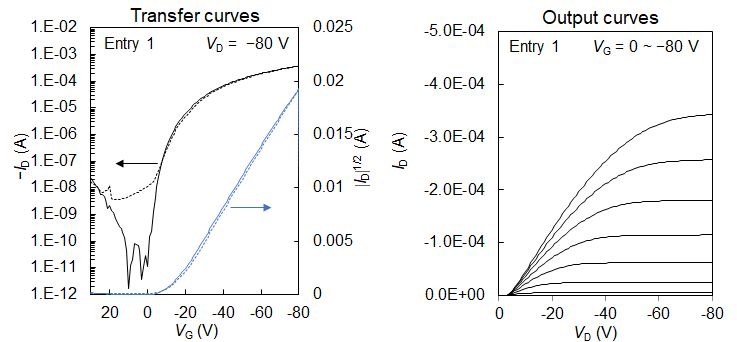
Figure. Transfer curves in the saturated region and output curves at different gate voltage
Experimental details
brication and evaluatio n of vacuum-deposited DPA [D5152]
< Substrate >
< Vacuum Deposition >
< Device Configuration >
< Evaluation Condition >
< Substrate >
- Bare Si/SiO2 (thickness of SiO2200 nm)
< Vacuum Deposition >
- Deposition rate of DPA [D5152] 0.3 Å/s, (under a pressure of -10−4 Pa)
- Substrate temperature during deposition: 50 °C
- Deposition rate of Au: 1.0 Å/s, (under a pressure of∼10 ∼10−4 Pa)
< Device Configuration >
- [n+-Si/SiO2 (200 nm) / DPA [D5152](50 nm) / Au (40 nm)]
- Top-Contact Bottom-Gate Type (TCBG)
- Channel Length: 50 μm
- Channel width: 1.5 mm
< Evaluation Condition >
- Under N2
- Field-effect mobilities (μ)) were determined from the transfer curves in the saturation regime using the following equation:
ID = (W/2L) μ Ci (VG − Vth)2