Published TCIMAIL newest issue No.196
Maximum quantity allowed is 999
Typical p-type material "pentacene”

Pentacene is one of the most typical P-type organic semiconductor material, and which has been studied actively in the field of organic electronics. Since the HOMO level of pentacene is higher than -5 eV, it is easily oxidized under ambient condition. Therefore, purification and preservation methods are important factor for the quality of pentacene.
We have commercialized "pentacene [P2524]" sublimed grade: excellent performance and high-mobility p-type OFET material, and also have studied fabrication and evaluation of OFET devices in our laboratory.
OFET performance evaluation of pentacene
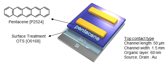
The field-effect mobility of pentacene was measured using the top-contact thin-film field-effect transistors geometry (Figure 1). The thin film of pentacene [P2524] as active layer (60 nm) was vacuum-deposited onto Si/SiO2 substrates (bare) or n-Octyltrichlorosilane (OTS) [O0168] -treated Si/SiO2 substrates at room temperature (Tsub = RT). The drain and source electrodes (40 nm) then were prepared by gold evaporation through a shadow mask on top of the pentacene film; the drain-source channel length (L) and width (w) are 50 μm and 1.5 mm, respectively. The characteristics of the OFET devices were measured under nitrogen conditions.

Figure 1. illustration for the device structure of pentacene-based OFET device
OFET Device performance
The performances of the OFET devices are summarized in Table 1 and figure 2. All pentacene -based devices exhibited pure typical p-channel field-effect transistor (FET) characteristics under nitrogen condition. The FET performance were significantly improved by self-assembled monolayer; the OTS-treated device demonstrated the highest performance with a hole carrier mobility of 1.52 cm2/Vs and an on/off ratio of 1.5 × 10⁷ (Figure 2).
![Figure2. Typical OFET characteristics of top-contact devices fabricated using pentacene[p0030]](/assets/cms-images/Typical-OFET-pentacene.png)
Figure 2. Typical OFET characteristics of top-contact devices fabricated using pentacene. (a, c) bare. (b, d) OTS-treated substrate. (a, b) Transfer curves in the saturated region. (c, d) Output curves at different gate voltages.

Table 1. OFET characteristics of pentacene
AFM images and XRD analysis
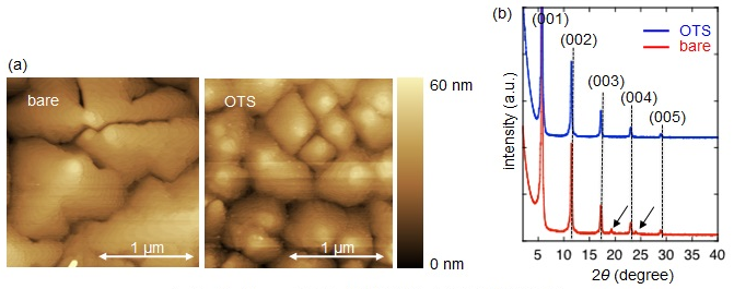
To clarify the pentacene thin film morphology and conformation, atomic force microscope (AFM) and X-ray diffraction (XRD) measurement were carried out. Regardless of bare or OTS-treated substrate, highly regular terrace structures were observed (Figure 3a). In addition, XRD measurements of the pentacene films showed a series of peaks assignable to (00h) reflections; and the diffraction peak at 2θ = 5.72° corresponds to a d-spacing of 15.5 Å (Figure 3b). These results showed that the pentacene molecules stood nearly perpendicular to the substrate (thin-film-phase) in the film form.

Figure3. AFM images (a) and XRD analysis (b) of pentacene filims
In the bare device (without SAM), two weak peaks assignable to face-on orientation were observed (Figure 3b, black arrow), which would create the disadvantage of carrier passes parallel to the substrate (Figure 4a). On the other hands, such peaks were not observed in the pentacene film on the OTS-treated substrate (Figure 3b). It is one reason why the mobility was higher in the OTS-treated OFET device.

Figure 4. Orientation images of pentacene thin film form
| ○ | A part of atomic force microscope (AFM: SPM-9700) was conducted at the AIST Nano-Processing Facility, supported by "Nanotechnology Platform Program" of the Ministry of Education, Culture, Sports, Science and Technology (MEXT), Japan. |
| ○ | A part of X-ray diffraction (XRD: Smart Lab) was conducted at Advanced Characterization Nanotechnology Platform of the University of Tokyo,supported by "Nanotechnology Platform" of the Ministry of Education, Culture, Sports, Science and Technology (MEXT), Japan. |

