Published TCIMAIL newest issue No.197
Maximum quantity allowed is 999
A ultra-high performance p-type semiconductor material "Ph-BTBT-10"
![A ultra-high performance p-type semiconductor material: Ph-BTBT-10 [D5491]](/assets/cms-images/d5491.jpg)
TCI has recently commercialized Ph-BTBT-10 as a ultra-high mobility and air stability p-type OFET material, and has begun fabrication and evaluation of Ph-BTBT-10-based OFET devices using by vacuum deposition methods in our laboratories. The devise showed a hole carrier mobility up to 14.0 cm2/Vs. Please see below for the details.
Fabrication and Evaluation of Ph-BTBT-10-based OFET Device
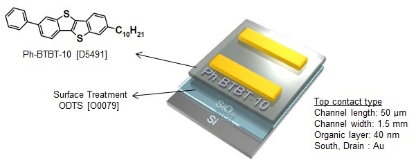
The field-effect mobility of Ph-BTBT-10 was measured using the top-contact thin-film field-effect transistors geometry (Figure 1). The thin film of Ph-BTBT-10 as the active layer (40 nm) was vacuum-deposited onto Si/SiO2 substrate (bare) or Octadecyltrichlorosilane (ODTS) [O0079]-treated Si/SiO2 substrate while heating the substrate. The drain and source electrodes (40 nm) then were prepared by gold evaporation through a shadow mask on top of the Ph-BTBT-10 film; the drain-source channel length (L) and width (w) are 50 µm and 1.5 mm, respectively. After deposition, these devices are thermal annealed at Tsub = 120 °C for 5 min under the ambient conditions, and the characteristics of the OFET devices were measured.

Figure 1. Illustration for the device structure of Ph-BTBT-10-based OFETs
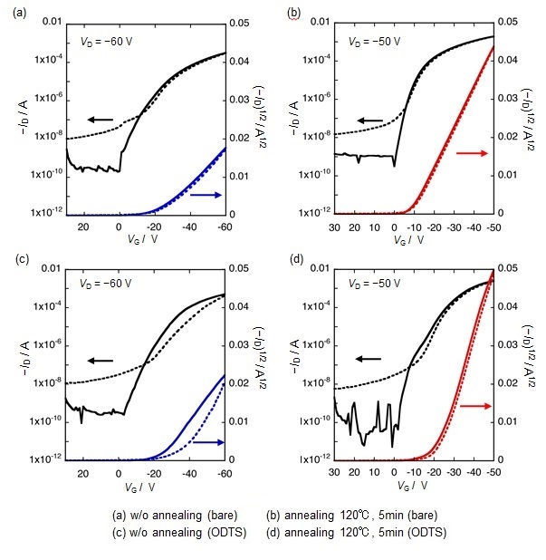
The performances of the OFET devices are summarized in Table 1 and Figure 2. All Ph-BTBT-10-based devices exhibited pure typical p-channel field-effect transistor (FET) characteristics. The FET mobilities were quite dependent on the thermal annealing treatment regardless of the self-assemble-monolayer (SAM) (Figure 2). This would be attributed to the phase transition from a monolayer to a bilayer crystal structure in the thin-film form.1)
The device fabricated on the bare substrate demonstrated good performance with a hole carrier mobility of 4.86 cm2/Vs and threshold voltage (Vth) of -8 V. Moreover, although Vth increased, the ODTS-treated devise showed the highest transport performance with a hole carrier mobility of 14.0 cm2/Vs. These results indicate that Ph-BTBT-10 can be handled through vacuum deposition methods, and it is a promising p-type OFET material possessing highly superior hole mobility. We demonstrated the top-ranked FET performances via vacuum deposition process using our in-house equipment.
Currently, we working on the optimization of device fabrication and investigating the correlation between device performance and the thin-film crystallinity.

Table 1. OFET characteristics of the Ph-BTBT-10-based devices

Figure 2. Transfer curves of the Ph-BTBT-10-based OFET devices

