

Published TCIMAIL newest issue No.197
Maximum quantity allowed is 999
Gelieve het aantal te selecteren
OFET Device Evaluation of π-Extended Rubrene Synthesized via Dearomative Annulative π-Extension (DAPEX) Reaction
Rubrene is one of the most frequently studied organic semiconductors (OSCs), and many derivatives have been synthesized and characterized as organic field-effect transistor (OFET) materials.1) However, to achieve π-extension of the poorly reactive tetracene core, it is necessary to functionalize the material in the early stage of the multi-step synthesis process. This has inevitably limited the diversity of rubrene-based OSCs. Recently, Itami's group have developed a dearomative annulative π-extension (DAPEX) reaction that realizes regioselective π-extension for nanocarbon compounds.2,3)By applying this DAPEX strategy to rubrene, a new type of rubrene derivative (1) with a π-extended tetracene core was synthesized in high yield (Fig. 1).4)
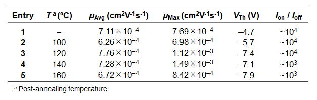
An OFET performance evaluation of 1 was carried out at TCI. The OFET device was fabricated by vacuum deposition, and exhibited good p-type semiconducting behavior, as shown in Figure 2. Table 1 shows the dependence of the OFET performance on the post- annealing temperature. The optimal annealing conditions were found to be 140 ºC for 15 min, with the resulting device exhibiting a maximum hole mobility of 1.49 × 10⁻³ cm2V-1s-1, which is comparable to that for rubrene-based devices. These results indicate that rubrene derivative (1) is a promising OSC for device applications. Also, the DAPEX reaction allows the production of chemically untapped OSCs having a larger acene core.

Figure 1. π-extension of runbrene via DAPEX reaction
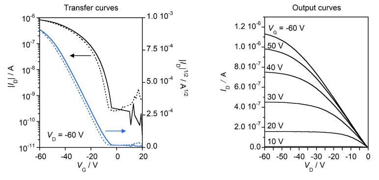
Figure 2. (a) Transfer and (b) output curves of rubrene derivative 1-based device
Table 1. OFET performances of rubrene derivative 1 –based devices
OFET device fabrication procedure
- ODTMS [O0256] SAM was formed on Sin++ / SiO2 (200 nm) substrate
- Boiling cleaning (IPA, 3 min)
- Vacuum deposition of π-extended rubrene (1)
Substrate temperature during deposition: RT
Deposition rate: 0.15 Å/sec
Film thickness: 40 nm - Vacuum deposition of Au electrode
Thickness: 40 nm
Channel length: 50 μm
Channel width: 1.5 mm - Thermal annealing in nitrogen glove box (100~160 ºC, 15 min)
- Device performance evaluation in a nitrogen glove box.
Octadecyltrimethoxysilane (ODTMS) SAM treatment procedure5)
- Piranha etching (H2SO4:H2O2 = 4:1, 80 ºC, 2 h)
- Ultrasonication (Deionized water, Acetone, IPA, 10 min each)
- Exposure to boiling vapor (IPA, 3min)
- UV/O3 treatment (1 h)
- Spin-coating of ODTMS [O0256]solution (3 mM trichloroethylene, 3000 RPM, 60 sec)
- Exposure to ammonium vapor (The substrates were placed together in a desiccator with a vial of ammonium hydroxide for 16 h)
- Ultrasonication (toluene, acetone, IPA, 10 min each)
References
- 1) Synthesis and Crystal Engineering of Rubrene and Its Derivatives
- 2) One-shot K-region-selective annulative π-extension for nanographene synthesis and functionalization
- 3) Diversity-oriented synthesis of nanographenes enabled by dearomative annulative π-extension
- 4) π-Extended Rubrenes via Dearomative Annulative π-Extension Reaction
- 5) Crystalline Ultrasmooth Self-Assembled Monolayers of Alkylsilanes for Organic Field-Effect Transistors
Related products
Material purity is an important factor directly influencing their OFET device parameters.
To check and enhance the quality and purity of the transistor materials, TCI has recently begun the fabrication and evaluation of the OFET devices using our products. We always seek to improve our technology and skill in order to provide high-purity and quality materials.