Published TCIMAIL newest issue No.197
Maximum quantity allowed is 999
Merci de sélectionner la quantité
Fabrication and Evaluation of Organic Field-Effect Transistors (OFETs) : anti-DMADT
![anti-DMADT [D4617]](/structure-300/D4617.jpg)
2,8-Dimethylanthra[2,3-b:6,7-b']dithiophene (purified by sublimation)
anti-DMADT
CAS RN: 1019983-99-3
Product Number: D4617
Performance of anti-DMADT [D4617]-based OFETs
![Fabrication method and evaluation of vacuum-deposited anti-DMADT [D4617]](/assets/cms-images/D4617-device-method-structure-en.png)
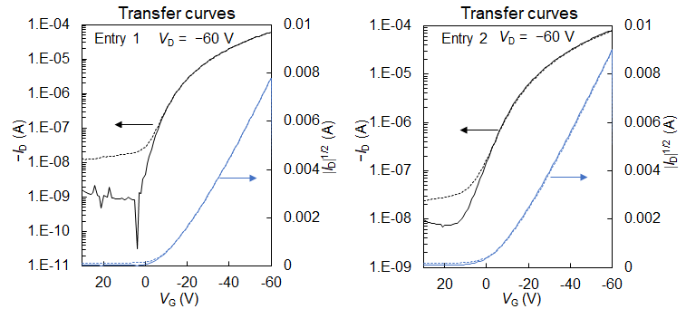
Table. OFETs Characteristics of anti-DMADT [D4617]
| Entry | Fabrication Method | Device Configuration | SAM Treatment | Tsub (°C) | Annealing Temp.a (°C) | Polarity | μ (cm2 V−1 s−1) | Vth (V) | Ion/Ioff |
|---|---|---|---|---|---|---|---|---|---|
| Entry1 | Fabrication MethodVacuum deposition |
Device ConfigurationTCBG | SAM Treatmentw/o Bare |
Tsub (°C)RT | Annealing Temp.a (°C)w/o | Polarityp | μ (cm2 V−1 s−1)0.11 | Vth (V)‒14 | Ion/Ioff104 |
| Entry2 | Fabrication MethodVacuum deposition |
Device ConfigurationTCBG | SAM Treatmentw/o Bare |
Tsub (°C)RT | Annealing Temp.a (°C)120 | Polarityp | μ (cm2 V−1 s−1)0.11 | Vth (V)‒7.7 | Ion/Ioff104 |

Figure. Transfer curves in the saturated region
Experimental details
Fabrication and evaluation of spin-coated anti-DMADT [D4617]-based OFETs
< Substrate>
< Substrate>
- Bare Si/SiO2 (thickness of SiO2: 200 nm)
- Deposition rate of anti-DMADT [D4617] 0.3 Å/s (under a pressure of∼10−4 Pa)
- Substrate temperature during deposition: RT
- Deposition rate of Au: 1.0 Å/s (under a pressure of∼10−4 Pa)
- Annealing condition: 120 ºC, 5 min, N2
- [n+-Si/SiO2 (200 nm) / anti-DMADT [D4617] (60 nm) / Au (40 nm)]
- Top-Contact Bottom-Gate Type (TCBG)
- Channel Length: 50 μm
- Channel width: 1.5 mm
- Under N2
- Field-effect mobilities (μ) were determined from the transfer curves in the saturation regime using the following equation: ID = (W/2L) μ Ci (VG − Vth)2

